
MSBTE
I Scheme Practice MCQs of “Digital Techniques (22320)”
All
Chapter MCQ.
Q1. The binary
number 10101 is equivalent to decimal number …………..
1. 19
2. 12
3. 27
4. 21
Answer : 4
Q2. The universal
gate is ………………
1. NAND gate
2. OR gate
3. AND gate
4. None of the above
Answer : 1
Q3. The inverter is
……………
1. NOT gate
2. OR gate
3. AND gate
4. None of the above
Answer : 1
Q4. The inputs of a
NAND gate are connected together. The resulting circuit is ………….
1. OR gate
2. AND gate
3. NOT gate
4. None of the above
Answer : 3
Q5. The NOR gate is
OR gate followed by ………………
1. AND gate
2. NAND gate
3. NOT gate
4. None of the above
Answer : 3
Q6. The NAND gate
is AND gate followed by …………………
1. NOT gate
2. OR gate
3. AND gate
4. None of the above
Answer : 1
Q7. Digital circuit
can be made by the repeated use of ………………
1. OR gates
2. NOT gates
3. NAND gates
4. None of the above
Answer : 3
Q8. The only
function of NOT gate is to ……………..
1. Stop signal
2. Invert input signal
3. Act as a universal gate
4. None of the above
Answer : 2
Q9. When an input
signal 1 is applied to a NOT gate, the output is
………………
1. 0
2. 1
3. Either 0 & 1
4. None of the above
Answer : 1
Q10. In Boolean
algebra, the bar sign (-) indicates ………………..
1. OR operation
2. AND operation
3. NOT operation
4. None of the above
Answer : 3
Q11. The resolution
of an n bit DAC with a maximum input of 5 V is 5 mV. The value
of n is …….
1. 8
2. 9
3. 10
4. 11
Answer : 3
Explanation:
(5/2N-1)1000 = 5 or N = 10
Q12. 2’s
complement of binary number 0101 is ………..
1. 1011
2. 1111
3. 1101
4. 1110
Answer : 1
Explanation: 1’s complement of 0101 is 1010
and 2’s complement is 1010+1 = 1011.
Q13. An OR
gate has 4 inputs. One input is high and the other three are low. The output
is …….
1. Low
2. High
3. alternately high and low
4. may be high or low depending
on relative magnitude of inputs
Answer : 2
Explanation: In OR any input high means
high output.
Q14. Decimal
number 10 is equal to binary number ……………
1. 1110
2. 1010
3. 1001
4. 1000
Answer : 2
Explanation: 1010 = 8 + 2 = 10 in decimal.
Q15. Both OR
and AND gates can have only two inputs.
1. True
2. False
Answer : 2
Explanation: Any number of inputs are
possible.
Q16. A device
which converts BCD to seven segments is called ……..
1. Encoder
2. Decoder
3. Multiplexer
4. None of these
Answer : 2
Explanation: Decoder converts binary/BCD to
alphanumeric.
Q17. In 2’s
complement representation the number 11100101 represents the decimal number
……………
1. +37
2. -31
3. +27
4. -27
Answer : 4
Explanation:
A = 11100101.
Therefore Ā = 00011010 and A’ = Ā + 1 = 00011011 = 16 + 8 + 2 + 1 =
27. Therefore A = -27.
Q18. A decade
counter skips ………..
1. binary states 1000 to 1111
2. binary states 0000 to 0011
3. binary states 1010 to 1111
4. binary states 1111 to higher
Answer : 3
Explanation: A decade counter counts
from 0 to 9. It has 4 flip-flops. The states skipped are 10 to 15 or 1010 to
1111.
Q19. BCD input
1000 is fed to a 7 segment display through a BCD to 7 segment decoder/driver.
The segments which will lit up are ………….
1. a, b, d
2. a, b, c
3. all
4. a, b, g, c, d
Answer : 3
Explanation: 1000 equals decimal 8
Therefore all segments will lit up.
Q20. A ring
counter with 5 flip flops will have ………. states.
1. 5
2. 10
3. 32
4. Infinite
Answer : 1
Q21. For the
gate in the given figure the output will be ………..
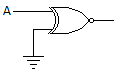
1. 0
2. 1
3. A
4. Ā
Answer : 4
Explanation: If A = 0, Y = 1 and A = 1,
Y = 0 Therefore Y = Ā.
Q22. In the
expression A + BC, the total number of minterms will be ………
1. 2
2. 3
3. 4
4. 5
Answer : 4
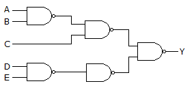
Q23. The
circuit in the given figure is a ………… gate.
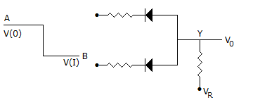
1. positive logic OR gate
2. negative logic OR gate
3. negative logic AND gate
4. positive logic AND gate
Answer : 2
Explanation: Since V(1) is lower state
than V(0) it is a negative logic circuit. Since diodes are in parallel, it is
an OR gate.
Q24. Which of
the following is non-saturating?
1. TTL
2. CMOS
3. ECL
4. Both 1 and 2
Answer : 3
Q25. The
number of digits in octal system is ………
1. 8
2. 7
3. 9
4. 10
Answer : 1
Explanation: The octal system has 8
digits 0 to 7.
Q16.
Answer : 2
Explanation:
Q26. The
access time of a word in 4 MB main memory is 100 ms. The access time of a word
in a 32 kb data cache memory is 10 ns. The average data cache bit ratio is
0.95. The efficiency of memory access time is ………
1. 9.5 ns
2. 14.5 ns
3. 20 ns
4. 95 ns
Answer : 2
Explanation: Access time = 0.95 x 10 +
0.05 x 100.
Q27. The
expression Y = pM (0, 1, 3, 4) is …………..
1. POS
2. SOP
3. Hybrid
4. none of these
Answer : 1
Explanation: This is a product of
sums expression.
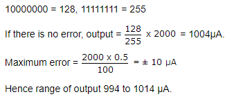
Q28. An 8 bit
DAC has a full scale output of 2 mA and full scale error of ± 0.5%. If input is
10000000 the range of outputs is ………….
1. 994 to 1014 μA
2. 990 to 1020 μA
3. 800 to 1200 μA
4. none of the above
Answer : 1
Explanation:
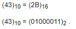
Q29. Decimal
43 in hexadecimal and BCD number system is respectively……. and ……..
1. B2 and 01000011
2. 2B and 01000011
3. 2B and 00110100
4. B2 and 01000100
Answer : 2
Explanation:
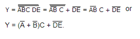
Q30. The
circuit of the given figure realizes the function …………
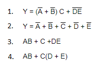
Answer : 1
Explanation:
Q31. An AND
gate has two inputs A and B and one inhibit input 3, Output is 1 if
1. A = 1, B = 1, S = 1
2. A = 1, B = 1, S = 0
3. A = 1, B = 0, S = 1
4. A = 1, B = 0, S = 0
Answer: 2
Explanation: All AND inputs must be 1 and inhibit 0
for output to be 1.
Q32. The
greatest negative number which can be stored is 8 bit computer using 2’s
complement arithmetic is ……..
1. -256
2. -128
3. -255
4. -127
Answer: 2
Explanation: The largest negative number is 1000
0000 = -128.
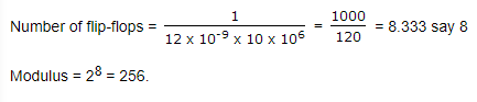
Q33. A JK flip
flop has tpd= 12 ns. The largest modulus of a ripple
counter using these flip flops and operating at 10 MHz is ……..
1. 16
2. 64
3. 128
4. 256
Answer: 4
Explanation:
Q34. The basic
storage element in a digital system is ………….
1. flipflop
2. counter
3. multiplexer
4. encoder
Answer : 1
Explanation: Storing can be done only in memory
and flip-flop is a memory element.
Q35. In a
ripple counter,
1. whenever a flipflop sets to 1,
the next higher FF toggles
2. whenever a flipflop sets to 0,
the next higher FF remains unchanged
3. whenever a flipflop sets to 1,
the next higher FF faces race condition
4. whenever a flipflop sets to 0,
the next higher FF faces race condition
Answer : 1
Explanation: In a ripple counter the effect ripples
through the counter.
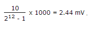
Q36. A 12 bit
ADC is used to convert analog voltage of 0 to 10 V into digital. The resolution
is ……….
1. 2.44 mV
2. 24.4 mV
3. 1.2 V
4. none of these
Answer : 1
Explanation:
Q37. For the
truth table of the given figure Y = ………….
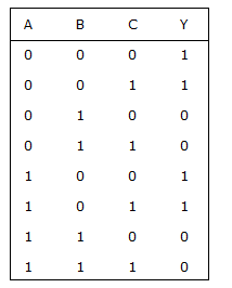
1. A + B + C
2. Ā +BC
3. Ā
4. B¯
Answer : 4
Explanation:

Q38. A full
adder can be made out of …………
1. two half adders
2. two half adders and a OR gate
3. two half adders and a NOT gate
4. three half adders
Answer : 2
Q39. If the
functions w, x, y, z are as follows
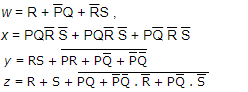
1. w = z x = z
2. w = z, x = y
3. w = y
4. w = y = z
Answer : 1
Q40. The
output of a half adder is ……….
1. Sum
2. Sum and Carry
3. Carry
4. none of these
Answer: 2
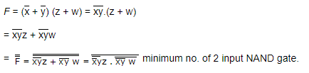
Q41. Minimum
number of 2-input NAND gates required to implement the function F =
(x + y) (Z + W) is ………..
1. 3
2. 4
3. 5
4. 6
Answer : 2
Explanation:
Q42. Which
device has one input and many outputs?
1. Multiplexer
2. Demultiplexer
3. Counter
4. Flip flop
Answer: 2
Explanation: Demultiplexer takes data from one line
and directs it to any of its N output depending on the status of its select
lines.
Q43. A carry
look ahead adder is frequently used for addition because
1. it costs less
2. it is faster
3. it is more accurate
4. uses fewer gates
Answer: 2
Explanation:
Q27.
Answer : 1
Explanation: In look ahead carry adder the
carry is directly derived from the gates when original inputs are being added.
Hence the addition is fast. This process requires more gates and is costly.
Q44. The
counter in the given figure is ………….
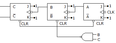
1. Mod 3
2. Mod 6
3. Mod 8
4. Mod 7
Answer : 2
Explanation: When counter is 110 the counter
resets. Hence mod 6.
Q45. In
register index addressing mode the effective address is given by ……..
1. index register value
2. sum of the index register
value and the operand
3. operand
4. difference of the index
register value and the operand
Answer : 2
Explanation:
4 = 22, in up scaling digit will be shifted by two bit in
right direction.
Q46. 7BF16 =
__________ 2
1. 0111 1011 1110
2. 0111 1011 1111
3. 0111 1011 0111
4. 0111 1011 0011
Answer : 2
Explanation:
7BF16 = 7 x 162 + 11 x 161 + 15 x 160 = 1983 in
decimal = 0111 1011 1111 in binary.
Q47. For the
minterm designation Y = ∑ m (1, 3, 5, 7) the complete expression is …………..
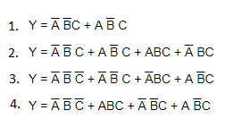
Answer : 2
Explanation:
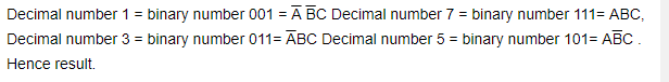
Q48. Zero suppression is not used
in actual practice.
1. True
2. False
Answer: 2
Explanation: Zero suppression is commonly used.
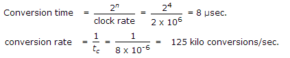
Q49. A counter
type A/D converter contains a 4 bit binary ladder and a counter driven by a 2
MHz clock. Then conversion time is ………..
1. 8 μ sec
2. 10 μ sec
3. 2 μ sec
4. 5 μ sec
Answer : 1
Explanation:
Q50. The
hexadecimal number (3E8)16 is equal to decimal number ………
1. 1000
2. 982
3. 768
4. 323
Answer : 1
Explanation: 3 x 162 + 14 x 161 +
8 = 1000
3rd sem electronics and telecommunications
ReplyDelete👍🏻👍🏻👌👌
ReplyDeleteThis comment has been removed by the author.
ReplyDeleteElectrical 3rd semester mcq please
ReplyDelete3 rd seam information technology
ReplyDelete3rd sem mechanical engineering
ReplyDelete3rd semester co
ReplyDeleteThis comment has been removed by the author.
ReplyDelete